Passive Components
Description
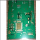
Multilayer PCB
Feature:
1) Layers: 1L-28L
2) Material: FR-4, CEM-1, CEM-3, High TG, FR4 Halogen Free,
3) Board finished thickness: 0.2mm-7.0mm
4) Solder mask color: green/yellow/black/white/red/blue
5) Max. finished board size: 23 × 25 ( 580mm×900mm )
6) Min. Line width: 3mil (0.075mm)
Min.Line spacing: 3mil (0.075mm)
7) Min. drilled hole size: 3mil (0.075mm)
8) Surface finish/treatment : HASL / HASL lead free, HAL, Chemical tin, Chemical Gold, mmersion Silver/Gold,OSP,Gold plating
9) Copper thickness: 0.5-7.0 OZ
10) Copper thickness in hole: >25.0μm (>1mil)
11) Inner packing: Vacuum packing / Plastic bag
Outer packing: Standard carton packing
12) Shape tolerance: ±0.13
Hole tolerance: PTH: ±0.076 NPTH: ±0.05
13) Certificate: UL, ISO 9001, ISO 14001, SGS, RoHS
14) Special requirements: Buried and blind vias+controlled impedance+BGA
15) Profiling: Punching, Routing, V-CUT, Beveling
16) Provides OEM services to all sorts of printed circuit board assembly as well as electronic encased products
Read More
Previous
board used for Cell...
Weiyuanda Industry Group Limited
PCB,PCBA
Address: Room 305 Section A Huameiju Business Centre Baoan District Shenzhen City Guangdong China ,
shenzhen, Guangdong
China, 518000
Tel: 86-0755-27757072
Fax:


