Electronic & Electrical
Description
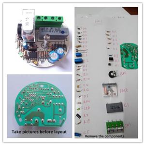
1. Real sample2. Schematic diagram and Overall configurations1.Take pictures before layout2.Remove the components from PCBA board, measure the parameter of components by digital electric bridge and multimeter.3.Grinding the solder mask on the pcb board4.Scan PCB wiring to the computer5.Adjust, copy the printing circuit board, then check and review.6.Do schematic diagram1.Fast PCB Fabrication for Samples and Mass Production2.Electronic Components Sourcing Servics3.PCBA Assembly Services:SMT,DIP,BGA...4.Function Test5.Stencil and Enclosure Assembly6.Standard Packing and On time Delivery1.Household Appliances2.Medical Products3.Automotive Products4.Industrial Products5.Communication Products(AVL/GPS/GSM Devices)6.Consumer Electronics ? ? ? ? ? ? ? ? ? ?1. How Many Layers are Best?Depending on the complexity of the overall circuitry being designed, a designer must decide how many layers the PCB should be.2. What service can we provide?We can provide PCB circuit board Gerber file layout, Copy and Clone,OEM and ODM service. Not only produce PCB,PCB Assembly,but also Plastic Enclosure,and Complete products. We can provide the manufacture pcb + purchase components + Assembly + Package one step service for our customers.
PCB Layout Design, Pcb Fabrication,Read More
Shenzhen Sunsoar Tech Co,Ltd
Key Word
Address: 4F, E block, Nanchang Huafeng,The Second Industrial Zone,Hangkong Road, Xixiang Town,Bao'an District, Shenzhen City, China,
shenzhen, guangdong
China, 518126
Tel: 86-755-82956801
Fax: 86-755-82954160


